

PCBA Surface Mount Technology SMT Processing OEM ODM

Contact Person : Ingrid
Phone Number : +86 18126235437
WhatsApp : +8618774804503

|
Detail Information |
|||
| High Light: | OEM DIP Insert Processing,ODM DIP Insert Processing,PCBA pcb designing and manufacturing |
||
|---|---|---|---|
Product Description
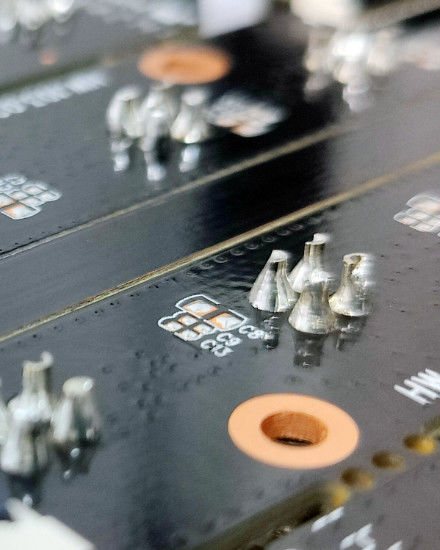
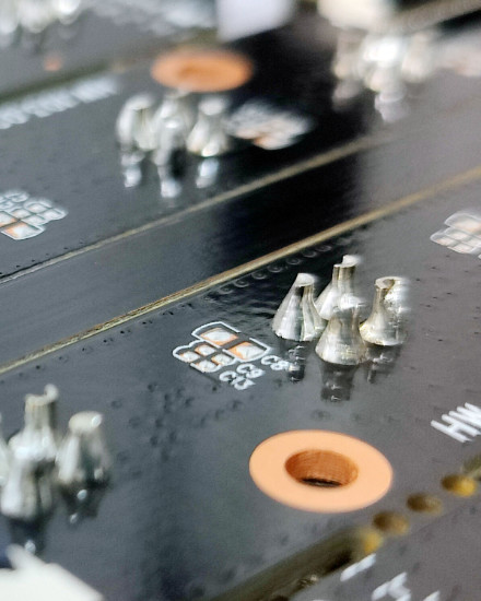
DIP (Dual In-Line Package) insert processing is a manufacturing technique used to insert through-hole components into a printed circuit board (PCB) that has pre-drilled holes. DIP components have leads or pins that extend from the bottom and are inserted through the holes in the PCB. The DIP insert processing typically involves the following steps:
1. PCB Preparation: The PCB is prepared for DIP component insertion. This involves ensuring that the PCB has pre-drilled holes in the correct locations and sizes to accommodate the DIP component leads.
2. Component Preparation: The DIP components are prepared for insertion. This may involve straightening or aligning the component leads to ensure they can be easily inserted into the PCB holes.
3. Insertion: Each DIP component is manually or automatically inserted into the corresponding holes on the PCB. The component leads are carefully aligned with the holes and inserted until the component body rests flush against the PCB surface.
4. Securing: Once the DIP components are inserted, they are secured to the PCB to ensure they remain in place during subsequent manufacturing processes and the product's lifecycle. This can be achieved through various methods, such as soldering, crimping, or using adhesive.
5. Soldering: After the DIP components are inserted and secured, the PCB is typically subjected to a soldering process to create reliable electrical connections. This can be done through wave soldering, selective soldering, or hand soldering, depending on the production setup and requirements.
6. Inspection: Once soldering is complete, the PCB undergoes inspection to verify the quality of the solder joints and component placement. Visual inspection, automated optical inspection (AOI), or other testing methods may be employed to detect any defects, misalignments, or soldering issues.
7. Testing: The assembled PCB, with the inserted and soldered DIP components, may undergo functional or electrical testing to ensure it meets the required specifications and performs as intended.
8. Final Assembly: After testing, the PCB may proceed to final assembly, where additional components and processes are added to complete the product.
DIP insert processing is commonly used for components that cannot be mounted using surface mount technology (SMT) or for applications where through-hole components are preferred due to their robustness or specific electrical requirements.
Enter Your Message
| Golden Triangle Group Ltd |
| Address: 4F, No.5 Building, Dingfeng Technology Park, Shayi Community, Shajing Town, Baoan District, Shenzhen, Guangdong Province, China |
| 86-0755-85275761 |
| sales27@gtpcb.com |