PCBA Assemble Manufacturing OEM Electronic Blender Machine PCB PCBA
| Description |
Capability |
|
android PCBA motherboard
|
PCBA fluxgate driver sensor
|
|
power bank PCBA
|
PCBA for coffee machine
|
|
earphone PCBA
|
bl dc ceiling fan PCBA
|
|
PCBA supplier
|
touch switch PCBA
|
|
android PCBA
|
wireless charge PCBA
|
|
finest PCBA
|
PCBA software development
|
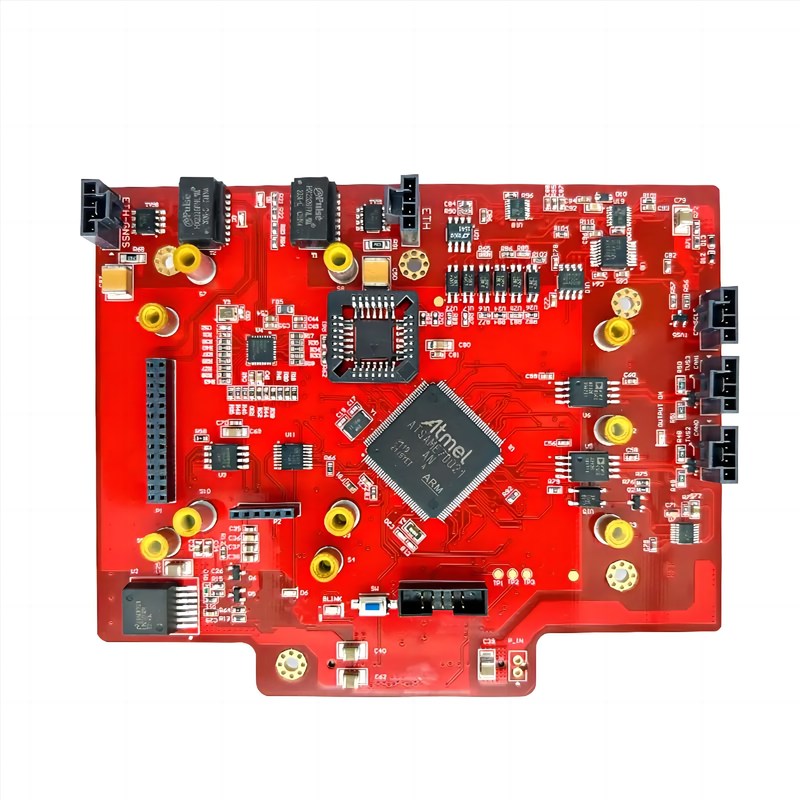
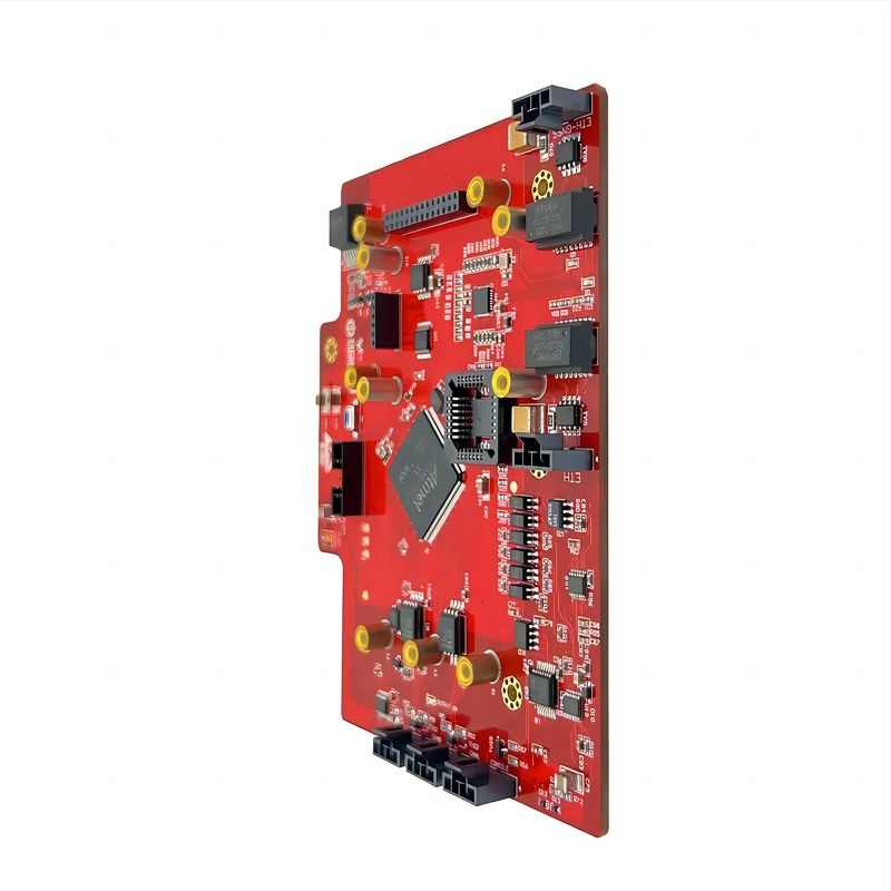
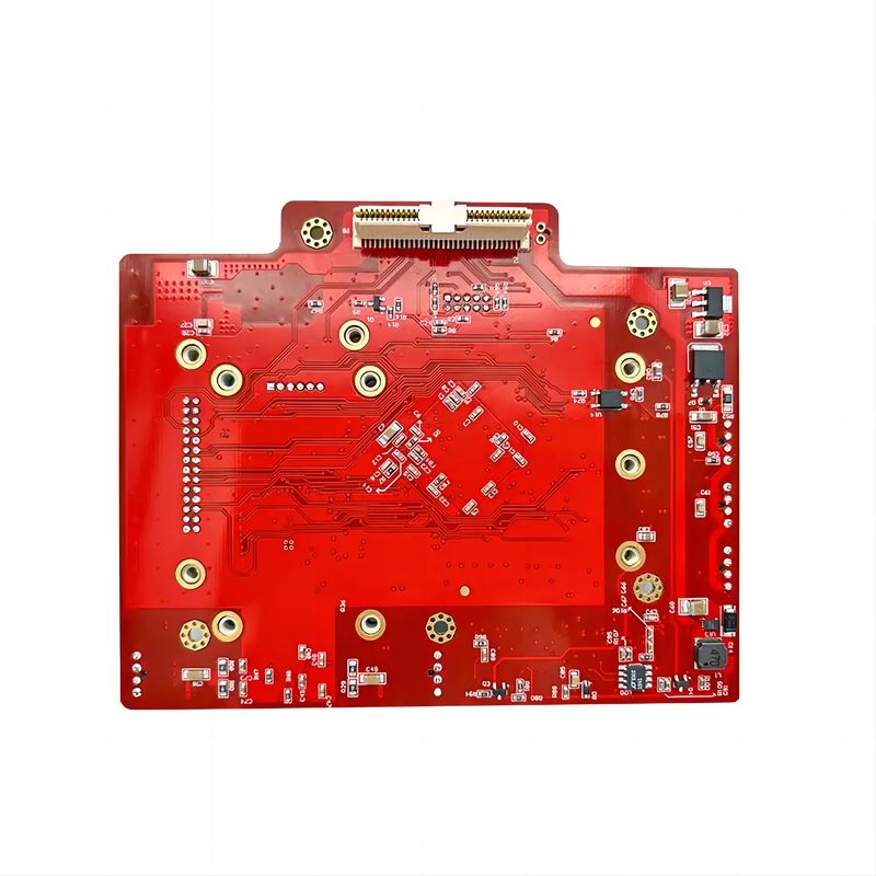
PCBA assembly manufacturing for an OEM electronic blender machine refers to the process of producing the printed circuit board assembly that controls and operates the blender. It involves designing the PCB, sourcing the components, assembling them onto the board, and conducting quality control checks. Here's a description of the key aspects of PCBA assembly manufacturing for an electronic blender machine:
PCB Design: The first step is to design the PCB layout for the electronic blender machine. The design takes into account the specific requirements of the blender, including the motor control, user interface, power management, and any additional features. The PCB layout is created using specialized software, considering factors such as signal integrity, component placement, and trace routing.
Component Sourcing: Once the PCB design is finalized, the manufacturer works with the OEM to source the required components for the PCBA assembly. This includes microcontrollers, integrated circuits, switches, connectors, capacitors, resistors, and other electronic components specified in the design. The manufacturer ensures the availability and quality of these components.
PCB Fabrication: The designed PCB layout is sent to a PCB fabrication facility. The facility manufactures the PCBs based on the design specifications, including the number of layers, copper thickness, solder mask, and silkscreen. The fabrication process involves etching copper layers, drilling holes, applying solder mask, and creating the necessary markings and labels.
Component Placement and Soldering: Once the fabricated PCBs are received, the manufacturing process moves to component placement and soldering. Automated or manual pick-and-place machines are used to accurately place the components onto the PCB, following the design's component placement guidelines. Surface mount technology (SMT) or through-hole technology (THT) techniques may be used, depending on the design requirements. The components are then soldered onto the PCB using reflow or wave soldering methods.

 Your message must be between 20-3,000 characters!